In between outdoor projects I've been tweaking the design of the Dual Class-A V2.0.
As promised I'm posting the schematic and some test results.
 Dual Class-A "DCAO 2" Headphone and Line Amplifier Schematic
Circuit Description
Dual Class-A "DCAO 2" Headphone and Line Amplifier Schematic
Circuit Description
Input is received by a THAT1240/1246 balanced line receiver.
Jumper J1 allows the second channel to be driven by the first channel either in or out of polarity.
J2 bypasses the THAT124X when balanced inputs are not required. When unbalanced, the line receiver IC is not inserted.
J3 selects either an on-board trimmer (T), fixed gain (F) and variable (V) using a front panel level control.
AC coupling is optional.
I'm considering a dual footprint for a 47 uF bipolar electrolytic or a 2u2 film with the bias resistor and op amp selected accordingly.
The output stage can run either open loop or closed depending on the jumper positions of J4 and J5.
For outputs up to about 65-100 mW, the heavy Class-A output current provides nearly identical performance open or closed.
Op amp B in the first group provides 12 dB gain and when feedback is global (output closed loop) serves as the error amplifier.
Jumper J4 bypasses op amp B to provide direct connection to the pre driver. This is ideal for unity gain line driver applications <100 mW.
When J5 is set in the local feedback position, op amp B provides gain.
When J5 is set in the global position feedback is taken from the output to extend the output power (in Class A/B) up to about 3W.
The 10 pF capacitor around op amp B assures that the error amp is slower than the output.
Op amp A and Q2 are the Vbe bias reference.
Q2 is mounted on the heatsink to provide thermal feedback.
Op amp B buffers the Vbe reference due to the high signal currents in the pre driver.
Op amps A and B in the second group emulate the THAT1646/DRV134 in the original Dual Class-A.
Op amp A sums the input signal and Vbe to drive the NPN output.
Op amp B differences the input signal and Vbe to drive the PNP output.
With no signal the NPN sees +Vbe; the PNP sees -Vbe.
The 200R trim balances the input drive signal of Q3 to match Q1.
This minimizes even-order THD contributions.
To adjust the trimmer J5 is set to "open loop," the output is loaded at about 100 mW, and the even order distortion nulled.
The 33R base resistors isolate the transistor base capacitance from the op amp outputs.
It was found that the OPA1612 and LME49720 benefited from having them.
Currently I'm using BD139/140s which have unspecified, but high, Cob. (Estimates run 100 pF).
The KSA1381/KSC3503 (2SA1381/2SC3503) at <3 pF might allow the 33Rs to be reduced somewhat.
At levels below 100 mW feedback isn't doing much.
The quiescent current is 100 mA and the output, even when open loop, is highly linear class-A.
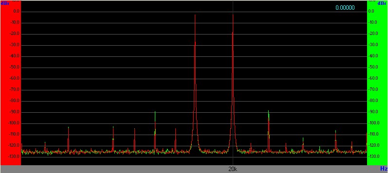
The following FFTs overlay the input (in green) over the output in red.
The vertical scale of the input has been adjusted to offset the +12 dB gain and attenuation in the analyzer input.
The first FFT is 65 mW at 10 kHz. The THD is estimated to be 0.0002%
 Dual Class-A 2 "DCAO2" 65mW 30R Load 10kHz Red is Output Green is Generator Monitor
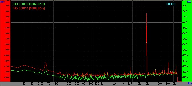
The next FFTs are at 1W at both 1 and 10 kHz:
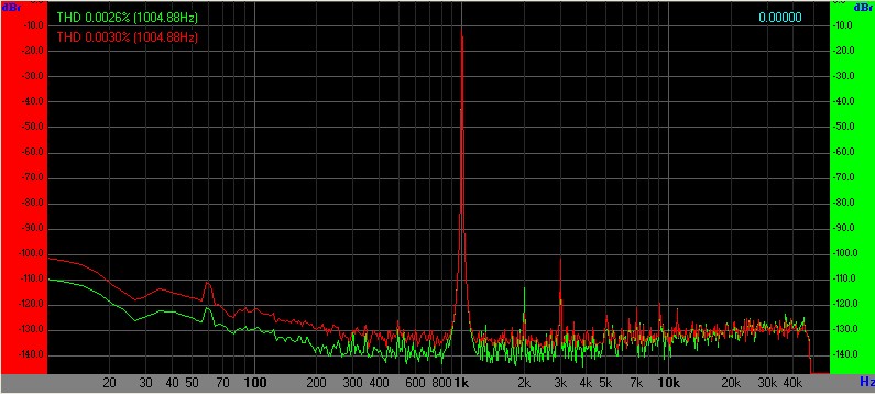 Dual Class-A 2 "DCAO2" 1W 30R Load 1 kHz Red is Output Green is Generator Monitor
The THD signature in the above shows that the DCAO2 is cancelling a bit of second harmonic. The THD is estimated to be 0.0004%
 Dual Class-A 2 "DCAO2" 1W 30R Load 10 kHz Red is Output Green is Generator Monitor
The THD at 10 kHz at 1W is estimated to be about 0.0038%.
I've spent a lot of time making the circuit work with a wide variety of op amps.
I don't recommend the NE5532/NJM2114 for the second group of op amps due to the "kink" in its gain/phase response.
When two 5532/2214 are cascaded inside the feedback loop there is significant response peaking.
Bandwidth is king for low THD in the second stage.
Op amps not having this kink, which are most, FETs and many BJT inputs work fine.
The OPA2134, OPA2604, OPA1612, OPA1642 and LME49720 all work very well.
My favorite is the OPA1612 with the LME49720 a close second.